

BEOL-compatible integration is a promising solution to the predicted performance challenges of future integrated circuits (ICs). It not only offers extreme miniaturisation and cost-effective fabrication of nanoelectronics devices including memory and processor enabling More than Moore products, but it also enables integrating additional functionalities such as photonic devices and various types of sensors onto Si based complementary metal oxide semiconductor (CMOS) ICs.
Case study 1
BEOL compatible and scalable integration of two dimensional (2D) transition metal dichalcogenide (TMD) based transistors
Quantum confinement effect is known to have significant impact on the electronic properties of low-dimensional materials with bandgap opening/widening as the key influential effect. Nevertheless, it could be employing for thin semimetal materials such as layered platinum diselenide (PtSe2) ultra-thin films, leading to opening bandgap with values comparable with conventional semiconductors in bulk form. In [2], L. Ansari et al., through collaborations with Trinity College Dublin and the group led by Dr Niall McEvoy, have demonstrated the quantum confinement effect in PtSe2 through both density functional theory (DFT) calculations and experimental characterisation of the large-area grown films with different thicknesses. The films which are grown with BEOL compatible thermally assisted conversion (TAC) process are used as channel material in the electronic switches fabricated through CMOS-compatible process steps such as photolithography and dry etching. Transfer characteristic of the field effect transistors is shown in Fig. 1 in addition to the DFT-predicted bandgap values benchmarked with other reported data in literature to date.
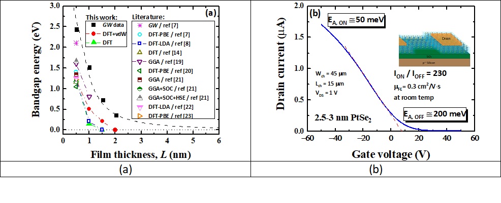
Fig. 1. (a) Bandgap energy versus PtSe2 film thickness from our DFT (solid green), DFT corrected by van der Waals interactions (solid red), and calibrated by GW calculations (solid black). See ref [2] for more details. (b) Room temperature transfer characteristic of a back-gated field-effect transistor (FET) device with a channel thickness of 2.5-3 nm PtSe2, a channel length of 15 µm, and channel width of 45 µm at VDS = 1 V. P-type characteristic and high ON/OFF ratio of 230 has been measured. Field-effect mobility is µFE = 0.3 cm2/V·s.
Case study 2
Full wafer integration through BEOL compatible direct wafer bonding
Monolithic integration of dissimilar materials by deposition of high-quality single crystalline layer onto Si is impeded by either large temperature process and/or lattice mismatch leading to a high density of threading dislocations in the epitaxial layer which would require high temperature post-growth annealing cycles. An alternative approach which avoids the epitaxial relationship and could be done with low thermal budget is direct wafer bonding followed by removal of all but a thin layer of the material being transferred. The technique (Smart CutTM) typically uses hydrogen implantation to form a sub-surface damaged layer which permits the separation (called exfoliation) of the top part of a wafer from its substrate after bonding. This technique does not require controlled wafer thinning as required with bulk wafer bonding.
Germanium (Ge) due to its compatibility with silicon processing is recognised as one of the best candidates for expanding the range of functions on CMOS-based devices and circuits. To investigate the direct wafer bonding integration technique, Ge/Si diodes have been fabricated through full-wafer BEOL- and CMOS-compatible processes. The p-type Ge substrate was implanted at room temperature with hydrogen ions to create a defective blistered region below the surface. Following the implant, the oxide layer was removed in a dilute hydrofluoric acid solution. An n+-Si host wafer and the p-Ge donor wafer were brought into proximity under vacuum once going through cleaning procedure. Wafer surfaces were then exposed to oxygen free radicals generated by a remote plasma ring prior to being brought into contact. The layer exfoliation was triggered by a short time (5 min) anneal at 300 °C after which a thin Ge film – 680 nm thick – remained bonded to the Si wafer. The electrical transport across the p-Ge/n+-Si junction was measured on a fabricated mesa structure (Fig. 2a and 2b) [3]. Similar fabrication approach of low-temperature direct wafer bonding has been developed to make Ge/Si photodiodes through controlled wafer thinning post bonding step. Responsivities in excess of 1 A/W at 1.55 μm are measured with a 5.4 μm thick Ge layer under surface-normal illumination (Fig. 2c). Capacitance-voltage measurements show that the interfacial band structure is dependent on both temperature and light level, moving from depletion of holes at −50 °C to accumulation at 20 °C, as shown in Fig. 2d. Interface traps filled by photo-generated and thermally-generated carriers are shown to play a crucial role. Their filling alters the potential barrier height at the interface leading to increased flow of dark current and the above unity responsivity.
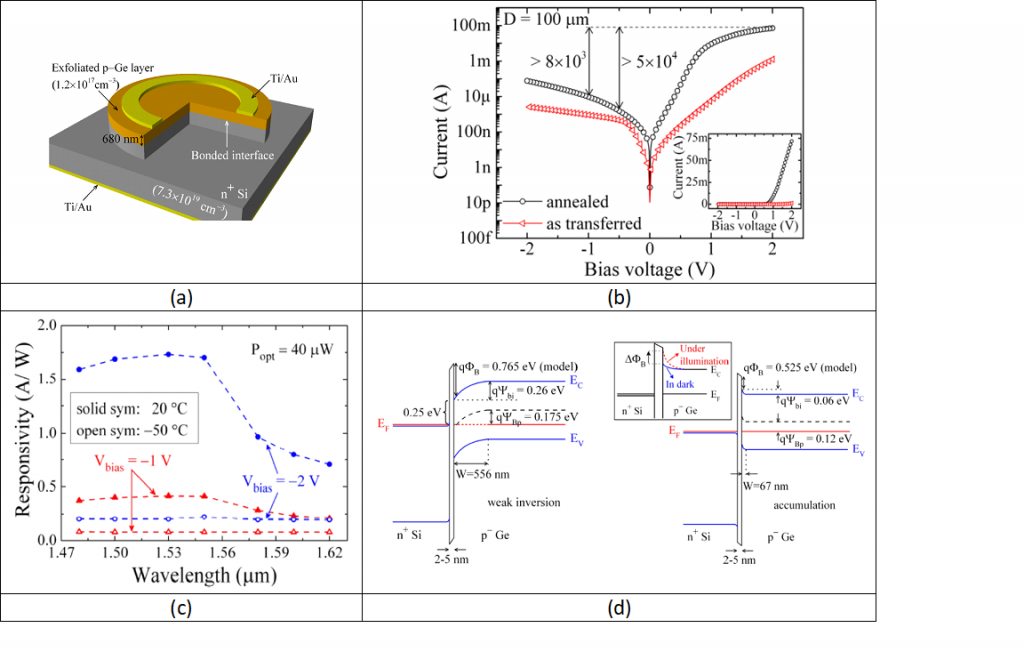
Fig. 2. (a) Schematic illustration of Ge/Si diode made by hydrogen implantation and layer transfer technique using direct wafer bonding. (b) IV characteristic of a 100 μm-diameter diode before and after annealing for 30 min at 400 °C in H2/N2 (0.05/0.95) atmosphere [3]. (c) Responsivity as a function of wavelength at a constant optical power of 40 μW at different reverse bias voltages and temperatures. (d) Schematic representation of the Ge/Si band diagram at equilibrium at (left) −50 °C, and (right) 20 °C. The inset of part (d) schematically illustrates the potential barrier lowering due to filling of acceptor traps by either temperature or light.
References
- F. Gity, F. Meaney, A. Curran, P. K. Hurley, S. Fahy, and L. Ansari, “Doping of Ultra-Thin Si Films: Combined First-Principles Calculations and Experimental Study”, Journal of Applied Physics, in press.
- L. Ansari, et al., “Quantum confinement-induced semimetal-to-semiconductor evolution in large-area ultra-thin PtSe2 films grown at 400 °C,” npj 2D Materials and Applications, 3, 33, 2019.https://doi.org/10.1038/s41699-019-0116-4
- F. Gity, et al., “Characterization of germanium/silicon p–n junction fabricated by low temperature direct wafer bonding and layer exfoliation,” Applied Physics Letters, 100, 092102, 2012.https://doi.org/10.1063/1.3688174
- F. Gity, et al., “Ge/Si heterojunction photodiodes fabricated by low temperature wafer bonding,” Optics Express, 21, 17309-17314, 2013 https://doi.org/10.1364/OE.21.017309