

Case Study
Device analysis by correlating electrical parameter extraction and electron microscopy
The IEEE International Roadmap for Devices and Systems (IRDS) for “More Moore” devices summarises the Logic Device state of the art where the FinFET is the key device architecture that could enable logic device scaling until 2025. Increasing fin height while reducing number of fins at unit footprint area is an effective solution to improve performance. It is forecasted that parasitics will remain as a dominant aspect in the performance of critical paths. Si has been scaled below 10 nm in multi-gate and silicon-on-insulator (SOI) device technologies, which poses Grand Challenges for device analysis at these dimensions. The introduction of new materials (Ge, strained Ge, III-V, high-k dielectrics…) and architectures (GeOI, Tunnel FETs and Nanowires) bring further challenges and require new techniques for parameter extraction and device characterisation.
For example, electrical dielectric thickness, interface state density, parasitic resistances, effective channel lengths, source and drain diffusions are critical to evaluate for device design, but are difficult to extract. However, through the judicious design and processing of electrical test structures and in combination with physics based modelling and simulation of their electrical properties many device parameters can be extracted enabling the understanding of the physical mechanisms controlling electron transport.
In parallel, electron microscopy provides direct measure of the physical dimensions of the devices and when applied with associated spectroscopy (EDX, EELS) can provide elemental and chemical information at the critical interfaces. However, conventional electron microscopy produces images that are two dimensional (2D) representation of three dimensional (3D) objects. Electron nano-tomography also known as 3D electron imaging enables researchers to visualise the real 3D shape of nanomaterials.
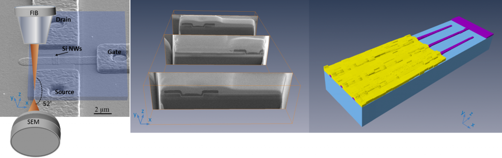
We have developed serial sectioning SEM/FIB tomography for 3D visualisation of materials and devices relevant to electronics and photonics. Briefly, serial sectioning SEM/FIB nanotomography uses finely controlled ion beam to mill away thin sections into the material volume while high resolution SEM is used to image obtained section at an oblique angle. Obtained set of images is used to reconstruct a 3D representation of the whole volume of the milled away material.
The Figure below shows an example of the application of this technique in solving performance issues with nanowire transistors produced by CMOS-compatible top down fabrication. This is of particular importance to microelectronics fabrication as the latest 22-nm note devices have truly 3D topology.
Reference
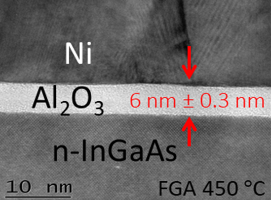
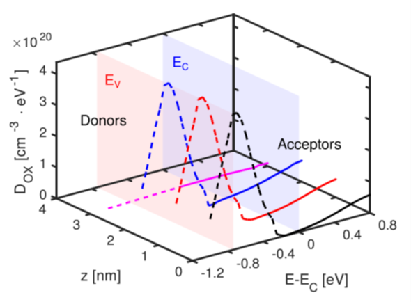
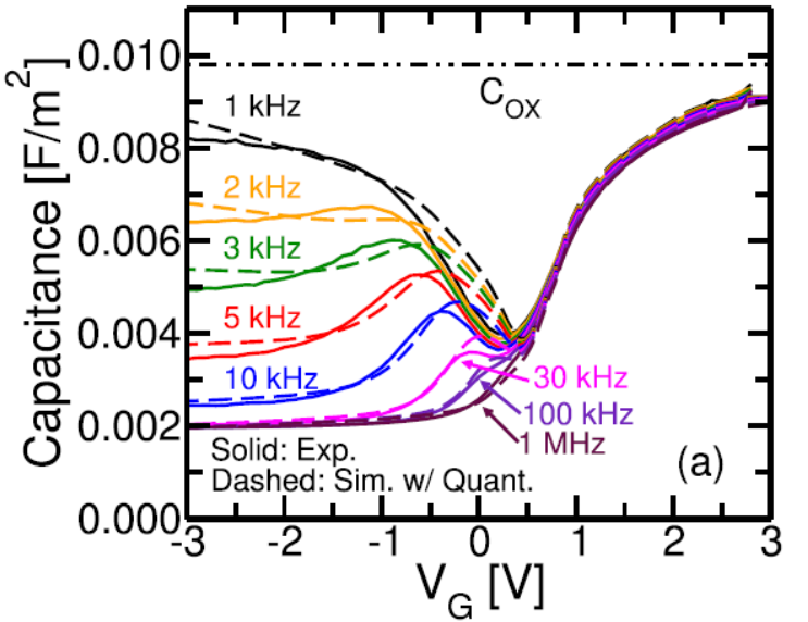
- E. Caruso, J. Lin, S. Monaghan, K. Cherkaoui, F. Gity, P. Palestri, D. Esseni, L. Selmi, and P. K. Hurley, “ The role of oxide traps aligned with the semiconductor energy gap in MOS systems,” IEEE Trans. Electron Devices 67, 4372 (2020). https://doi.org/10.1109/TED.2020.3018095