Our interest in semiconductor device fabrication is driven by the need to i) develop structures with sub-10 nm dimensions for future device nodes and ii) to introduce novel materials (Ge, GeSn, etc.) in the CMOS processing. Electron beam lithography (EBL) offers flexible but controlled way to fabricating prototype devices with varying architectures and dimensions down to few nm. We have developed fabrication work flows based on using high-resolution EBL resist, hydrogen silsesquioxane (HSQ), that has the advantage of extreme resolution and high etch resistance for a variety of substrates. A challenge with EBL/HSQ process is that the HSQ developer is a relatively concentrated base that is not always compatible with the underlying surface, typical example would be Ge. Hence, we have developed HSQ process flows that are compatible with a variety of challenging substrates and surfaces such as Ge, GeSn, NiSi, TiN, etc. Another challenge with HSQ patterning is the development of high-density (sub-20 nm pitch) structures due to high contribution of electron proximity effects. We have developed HSQ exposure workflows for incident beam energies ranging from 10 kV – 100 kV using two different EBL systems e.g. RAITH e-line and ElionixELS-G100. Inspired by the interest in developing contacts to nanowires, and in particular their separate facets, we were the first to develop a direct-write lithography process, based on EBID for contacting vertical ZnO wire facets. We have also used our lithography approaches to contact grown nanowires to demonstrate prototype nanowire FET devices with emerging channel materials such as Ge, GeSn.
Case study
High density/high fidelity line patterns for nanowire and fin FET devices
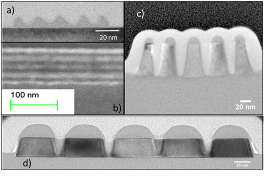
One of the key requirements in lithography is the development of extreme density (sub-20 nm pitch) patterned line structures and their pattern transfer via RIE. This is an extremely challenging task, with a major promise coming from the future EUV for mass fabrication. While EUV area is still far from practice, EBL offers the possibility to test resists and etching recipes by developing prototype structures and devices. However only few research groups have demonstrated EBL process flows for sub-20 nm pitch features worldwide, and to the best of our knowledge, there is no other nano-fabrication facility capable of routinely fabricating such dense patterns on large areas. While, we are capable of routinely fabricating widely spaced 7-8 nm line width structures, the repeatable patterning of extreme density patterns (Fig. 1a and 1b) showed to be very challenging. Our best results (obtained with good repeatability) now are at 25 nm pitch structures (Fig. 1c) with line widths of 12 nm and line spacing of 13 nm.

Fig. 1. 7-8 nm line width structures (a and b). (c) 25 nm pitch structures with line widths of 12 nm and line spacing of 13 nm.
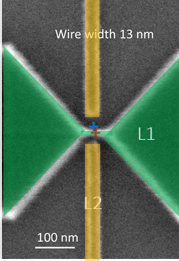
For the realisation split gate FET devices that can have novel application as NEMs resonators for quantum computing read out system we demonstrated EBL pattern-to-pattern alignment with accuracy close to 10 nm. See Fig. 2, Layer 1 of nanowire/pads (in green) is patterned first, followed by Layer 2 of split-gates (in yellow). The red and blue crosses depict the misalignment between intended and actual centres of Layer 2, measured misalignments in X and Y directions are lower than 10 nm. The alignment test is done by using four marks 2 mm apart in HSQ resist on Si.

Fig. 2. Realisation of split gate FET device. Layer 1 of nanowire/pads (in green) is patterned first, followed by Layer 2 of split-gates (in yellow). Slight misalignment of less than 10 nm in X and Y directions measured using the red and blue crosses.

