

The fabrication of electronic devices from nanostructures enables us to probe their functionality, and moreover to benchmark proposed novel materials from a variety of standpoints.
Recently, device miniaturisation has reached fundamental physical constraints, therefore substantial efforts are being made in defining the performance limits and exploring new applications to overcome this, including the development of devices based on 3D nanostructures, many fabricated from nanostructures such as bottom-up grown nanowires. In recent decades, advances in nanowire synthesis and fabrication have led to the development of devices such as field effect transistors, logic circuits, sensing devices and solar cells.
A typical process flow is shown in the schematic in Fig 1. The nanostructures in this case as bottom-up synthesised nanowires. Processes are developed for their transfer to a suitable substrate, lithography defined patterning, cleaning, and for contact metallisation. Finally the electronic devices can be measured electrically, in this case electrical current as function of applied gate voltage was the probed.
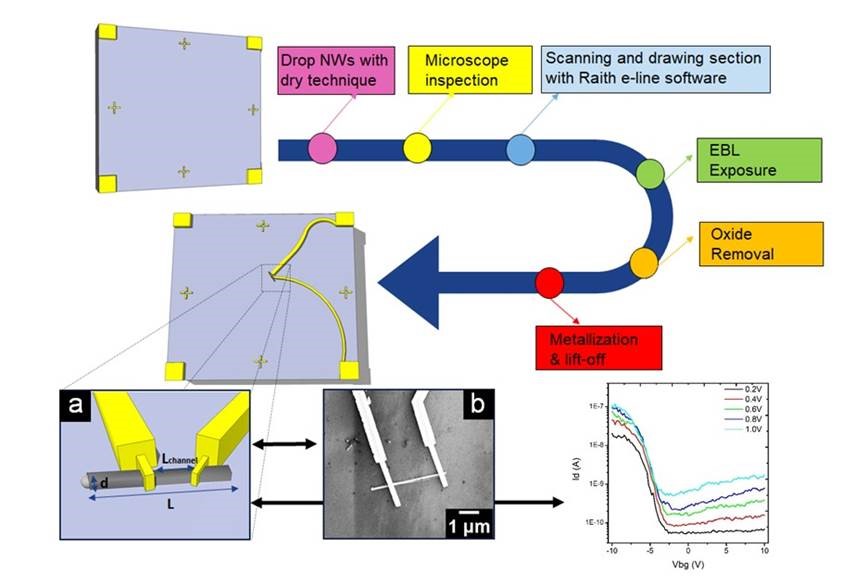
Fig. 1. Illustrative image of the contacting scheme for the bottom-up-grown nanowires (NWs) and device process flow. (a) Close-up schematic. (b) Representative SEM image. Electrical performance of a fabricated NW device is also shown.
Reference
- E. Galluccio, J. Doherty, S. Biswas, J.D. Holmes, R. Duffy, Field-Effect Transistor Figures of Merit for Vapor–Liquid–Solid-Grown Ge1-xSnx (x = 0.03–0.09) Nanowire Devices, ACS Appl. Electron. Mater. 2, 5, 1226 (2020) https://doi.org/10.1021/acsaelm.0c00036