
Continued scaling of semiconductor devices, the switch to complex three dimensional geometries and the expansion beyond CMOS, so-called More-Than-Moore, means that device processing is becoming more complicated, while we are at the point where every atom makes a difference and films can be at a thickness of approx. 1-2 nm. Thus, the need for atomic level control makes atomic level processing, exemplified by atomic layer deposition (ALD), atomic layer etching (ALE) and molecular layer deposition (MLD), absolutely necessary.
Since atomic level processing is driven by the chemistry of precursors at surfaces it is a natural candidate for atomic level modelling, using first principles density functional theory (DFT). DFT is able to model surfaces and surface chemistry to a reasonable level of accuracy, treating hundreds of atoms at a time. One can determine the thermodynamics of potential reactions and compute activation barriers for particular processes. These allow one to assess if the chemistry is feasible and what reaction by-products are possible. Furthermore, one can use activation barriers from DFT as input to kinetic Monte Carlo simulations to explore film growth on much larger and complex models, obtaining results that can be directly compared to experiment.
Our focus in the CMOS++ cluster is on plasma atomic layer deposition of metals, atomic layer deposition of nitrides as barrier and liner layers in transistors, atomic layer etching of high-k materials and metals and molecular layer deposition of hybrid organic-inorganic materials for low-k materials or encapsulation. Our work is supported by Science Foundation Ireland, Horizon 2020 MSCA ITN HYCOAT, Enterprise Ireland and direct industry support.
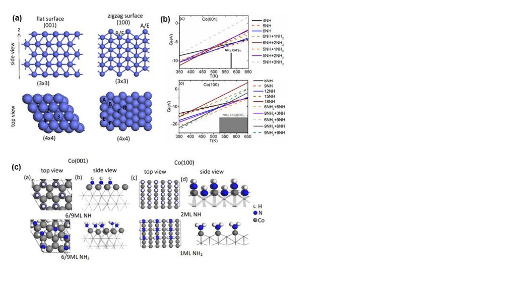
A recent highlight is modelling the metal pulse in the nitrogen plasma ALD of cobalt, which is of high importance in nanodevices, e.g. as interconnect metal showing lower resistivity than copper at small dimensions. We first determined structures cobalt surfaces terminated in NH and NH2 groups which are proposed to be present after the nitrogen/hydrogen plasma pulse (similar to production of surface –OH species in oxygen plasma ALD) and predicted the coverage of NH/NH2 under typical ALD operating conditions. Figure 1(a) shows the atomic structure of bare Co (001) and (100) surfaces, while Figure 1(b) shows how the stability of different coverages of NH and NH2 changes with temperature (the grey boxes show the typical experimental temperature ranges for Co ALD) and Figure 1(c) shows the atomic structures of Co (001) and (100) with NH and NH2 terminations.
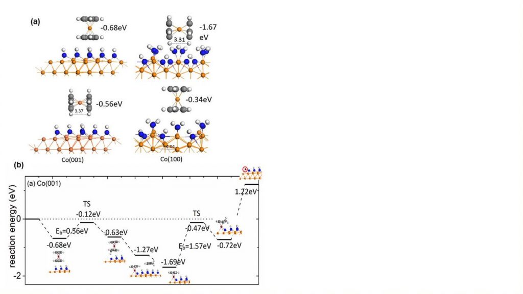
With these surface models we have investigated how the well-known Co(Cp)2 precursor interacts with the surface and the energy pathway to eliminate Cp ligands via hydrogen transfer from the surface to a Cp ring, releasing CpH. Figure 2(a) shows the Co(Cp)2 precursor interacting with the NHx-terminated Co surfaces to allow us predict the preferred orientation of the precursor; the preference depends on the surface structure and is driven by the geometry of the surface layer. Figure 2(b) shows the computed energy pathway for the elimination of Cp from the precursor, including the activation barrier for the first H transfer step. This barrier is rather moderate at 0.56 eV but the preference is for one Cp ligand to be eliminated, leaving CoCp on the surface. This analysis is extended to Ru ALD, following a similar approach.
We have presented some of the first DFT level studies of ALE of metal oxides and metals. This year, we investigated the ALE of crystalline ZrO2 and HfO2 high-k dielectrics using HF as the first reactant and Tungsten metal . In ALE, the concept is to use a reactive agent, such as HF, to modify the surface layer of the target material but this modification is not volatile. The second reagent can then undergo ligand exchange to produce volatile species which are removed during the purge and a layer (or partial layer) of the target material is thus removed. The concept of ALE is shown in Figure 3 (a). ALE can be thought of as the opposite of ALD (although it is more complex than this) and is expected to see wide use in the etching of thin films where the direct deposition of such thin films will be challenging.
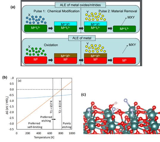
In Figure 3(b) we show our free energy profile predicted for the HF step in ALE of HfO2. We defined self-limiting etch as that process in which one layer of HfO2 is converted to the fluoride (HfF + H2O) and continuous etch as that process in which the entire HfO2 is converted to HfF. This plot allows us to predict the temperature at which the preference switches from self-limiting etch to continuous etch and therefore we predict HF ALE of HfO2 to be self-limiting up to approx. 650 K, consistent with experiment. Figure 3(c) shows the atomic structure when HF adsorbs at the HfO2 surface. We see that the HF molecule dissociates spontaneously to produce HfF and OH species showing high reactivity of this oxide to HF required for ALE.